In the heart of Canberra, a team of researchers led by Lachlan Oberg from the Department of Quantum Science and Technology at the Australian National University is pioneering a novel approach to quantum technology that could revolutionize the energy sector. Their work, published in the journal *Materials for Quantum Technology* (translated from the original title “Materials for Quantum Technology”), focuses on the nitrogen-vacancy (NV) center in diamond, a promising candidate for quantum information processing and metrology.
Quantum technologies, with their potential to process information at unprecedented speeds and sensitivities, are poised to transform industries ranging from computing to energy. However, the practical realization of large-scale quantum devices has been hindered by the limitations of current fabrication techniques. Oberg and his team are tackling this challenge head-on, proposing a bottom-up fabrication method that is scalable, deterministic, and possesses atomic-scale precision.
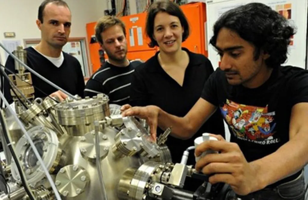
The team’s approach is inspired by existing methods for fabricating phosphorous defect qubits in silicon. They envision a technique called hydrogen depassivation lithography, which could enable the atomically-precise manufacturing of NV centers in diamond. This method involves using a scanning tunneling microscope (STM) to remove hydrogen atoms from the diamond surface, allowing nitrogen atoms to be incorporated into the diamond lattice with high precision.
“The potential of this technique lies in its scalability and precision,” Oberg explains. “By controlling the placement of NV centers at the atomic level, we can create large-scale quantum devices that harness the collective properties of multiple NV centers. This could enable room-temperature quantum computing and sensing, which would be a significant advancement for the field.”
The implications for the energy sector are substantial. Quantum sensing, for instance, could lead to the development of highly sensitive magnetic field detectors, which could be used to monitor the health of power grids and detect faults before they cause outages. Quantum computing, on the other hand, could optimize energy distribution networks, reducing waste and improving efficiency.
However, the path to commercialization is not without its challenges. The team identifies several key hurdles in the development of this technique, including the need for improved STM control and the development of methods to incorporate nitrogen atoms into the diamond lattice with high fidelity.
Despite these challenges, the team’s work represents a significant step forward in the quest for scalable quantum technologies. As Oberg notes, “This perspective article outlines a viable multi-step procedure for realizing scalable fabrication of diamond quantum devices. While there are challenges ahead, the potential benefits make this a promising avenue for future research.”
The research conducted by Oberg and his team could shape the future of quantum technology, bringing us closer to a world where quantum computing and sensing are not just theoretical concepts, but practical tools that drive innovation and efficiency in industries like energy. As the field continues to evolve, their work serves as a testament to the power of human ingenuity and the potential of quantum technologies to transform our world.