In the ever-evolving landscape of organic semiconductor technology, a groundbreaking approach is emerging that could revolutionize the way we manufacture and enhance the performance of these versatile materials. Researchers, led by Yueping Lai from the Key Laboratory of Green Chemistry & Technology at Sichuan University in China, have uncovered a novel method to regulate multiple properties of organic semiconductors using photo-crosslinkers in a process known as direct lithography. This innovation, detailed in a recent study published in the journal *Macromolecular Materials and Engineering* (which translates to *Macromolecular Materials and Engineering* in English), promises to streamline production processes and significantly boost the efficiency and stability of organic semiconductor devices.
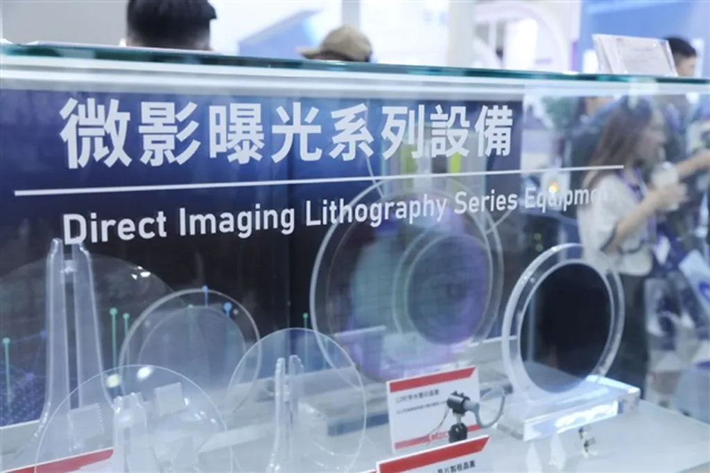
Traditional organic lithography processes are notoriously complex, involving multiple steps such as protection, baking, etching, and transfer. However, direct lithography simplifies this procedure to just three steps: spin-coating, exposure, and development. This simplification not only reduces the time and cost of production but also eliminates the need for intricate and often error-prone procedures. “The direct lithography process is a game-changer,” says Lai. “It allows us to achieve high-precision patterning of organic integrated circuits while simultaneously enhancing their performance attributes.”
The key to this innovation lies in the use of photo-crosslinkers, materials with negative photoresist characteristics that remain in the blended film after the lithography process. These photo-crosslinkers influence the crystalline structure and morphology of the semiconductor film, which in turn affects its tensile properties, charge carrier mobility, stability, and dielectric properties. “By designing the photo-crosslinker appropriately, we can effectively regulate and enhance these properties,” explains Lai. This dual functionality—patterning and performance enhancement—makes direct lithography a highly attractive option for the commercial production of organic semiconductor devices.
The implications for the energy sector are particularly significant. Organic semiconductors are already being explored for use in solar cells, organic light-emitting diodes (OLEDs), and other energy-efficient technologies. The ability to enhance the stability and efficiency of these devices through direct lithography could accelerate their adoption and improve their performance in real-world applications. “This approach could lead to more efficient and durable energy devices, which is crucial for the transition to renewable energy sources,” says Lai.
While the potential of direct lithography is immense, the field is still in its early stages. The study by Lai and his team provides a systematic summary and organization of the impact of photo-crosslinkers on semiconductors, offering valuable guidance for the design of novel photo-crosslinkers. “Systematic organization is crucial for the future development of direct lithography,” emphasizes Lai. This research not only highlights the current capabilities of direct lithography but also paves the way for future advancements in the field.
As the energy sector continues to seek innovative solutions to improve the efficiency and sustainability of energy technologies, the work of Yueping Lai and his team offers a promising path forward. By simplifying the production process and enhancing the performance of organic semiconductor devices, direct lithography could play a pivotal role in shaping the future of energy technology. The study, published in *Macromolecular Materials and Engineering*, serves as a testament to the ongoing innovation in this dynamic field, inspiring further research and development in organic semiconductor technology.