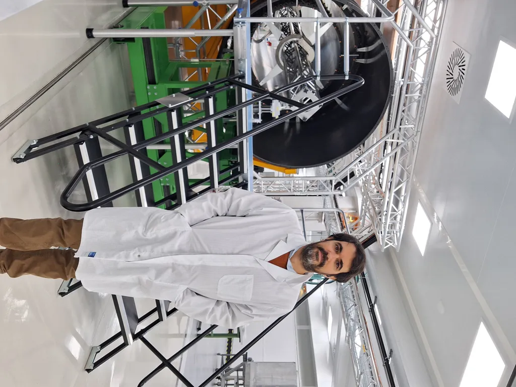
In a significant stride toward understanding and harnessing the unique properties of topological semimetals, researchers at the University of Warwick have unveiled new insights into the surface structure and growth challenges of Indium Bismuth (InBi). This work, led by Thomas J. Rehaag from the Department of Physics, could pave the way for innovative applications in the energy sector, particularly in advanced electronic and quantum computing technologies.
InBi is a semimetal that exhibits topologically non-trivial electronic surface states, making it a material of great interest for next-generation electronic devices. Its compatibility with conventional III-V semiconductors further enhances its potential for integration into existing technologies. However, the path to leveraging its full potential has been fraught with challenges, primarily centered around understanding its surface structure and achieving high-quality epitaxial growth.
The study, published in the journal “Materials Research Express” (which translates to “Materials Research Express” in English), reveals that the (001) cleave surfaces of InBi do not conform to the previously assumed single Bi-Bi cleave plane. Instead, they expose both Indium- and Bismuth-terminated surface regions. This discovery is crucial as it directly impacts the band structure studies and growth mechanisms of the material.
“Understanding the surface structure of InBi is fundamental to achieving high-quality epitaxial growth,” said Thomas J. Rehaag. “Our findings challenge the existing assumptions and provide a clearer picture of the surface composition, which is essential for advancing the growth techniques.”
The researchers employed ultra-high vacuum conditions to cleave the crystals and used them as substrates for ultra-low temperature homoepitaxy via periodic supply epitaxy (PSE). This method involves alternate fluxes of Bismuth and Indium. Despite their efforts, high-quality homoepitaxial growth of InBi was not achieved under these conditions. The study highlights the complexity and challenges involved in growing high-quality InBi epilayers beyond the ultra-thin heteroepitaxial layers recently demonstrated.
The 3D and 2D surface structures produced by PSE were meticulously studied using reflection high energy electron diffraction and atomic force microscopy. These techniques provided detailed insights into the surface morphology and structural properties, which are critical for optimizing growth conditions.
“This research underscores the need for further investigation into the growth mechanisms of InBi,” added Rehaag. “By addressing these challenges, we can unlock the full potential of this fascinating material for applications in advanced electronics and quantum computing.”
The implications of this research extend beyond the laboratory. InBi’s unique properties could revolutionize the energy sector by enabling more efficient and powerful electronic devices. As the world transitions towards renewable energy sources and advanced computing technologies, materials like InBi could play a pivotal role in shaping the future of energy storage, conversion, and distribution.
In conclusion, the work by Rehaag and his team at the University of Warwick represents a significant step forward in the understanding and development of topological semimetals. By shedding light on the surface structure and growth challenges of InBi, this research lays the groundwork for future advancements in the field. As the scientific community continues to explore the potential of these materials, the energy sector stands to benefit from the innovative technologies that may emerge.