In a significant stride towards enhancing indoor photovoltaic (PV) technology, researchers have identified a promising material that could revolutionize the way we power our indoor devices. The study, led by Mostafa Hamed from the Department of Engineering Physics and Mathematics, focuses on the all-inorganic CsPbIBr2 perovskite material, which shows remarkable potential for indoor applications.
The demand for efficient and stable energy sources for indoor use has been steadily rising, driven by the proliferation of Internet of Things (IoT) devices and the need for sustainable power solutions. Traditional solar cells, designed for outdoor use, often fall short in indoor environments due to their inability to harness the lower light intensities effectively. This is where CsPbIBr2 comes into play.
CsPbIBr2 exhibits a unique combination of properties that make it well-suited for indoor PV applications. “It has a wide direct bandgap of 2.05 eV, a high absorption coefficient, and excellent carrier mobilities,” explains Hamed. These characteristics enable the material to efficiently convert the photon energy from indoor lighting sources into electrical energy.
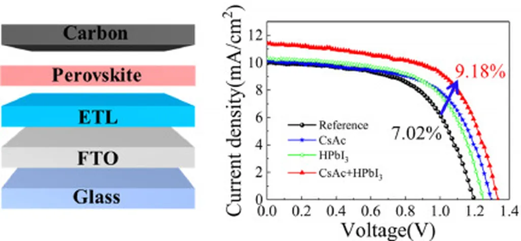
The research began with an experimental CsPbIBr2-based solar cell that demonstrated a power conversion efficiency (PCE) of 11.01% under 1-sun illumination. However, the team didn’t stop there. They employed the SCAPS-1D simulation tool to delve deeper into the material’s potential. By validating their simulation approach against experimental data, they identified a critical limitation in the single electron transport layer (ETL) design: suboptimal band alignment.
This insight led to a comprehensive optimization strategy. The team explored a double ETL configuration, analyzed optimal transport layer materials, and examined the impact of absorber layer thickness and defect concentrations. Through this methodical approach, they progressively enhanced the cell’s performance, achieving a remarkable 21.85% PCE under 200 lux, and a 2900 K indoor LED illumination.
The implications of this research are profound for the energy sector. Indoor PV technology has the potential to power a wide range of devices, from sensors and actuators to smart home systems, without the need for batteries or external power sources. This could lead to significant cost savings, reduced environmental impact, and enhanced convenience for consumers.
As Hamed notes, “The simulation results provided in this study reveal the prospective of CsPbIBr2 PSCs as a promising candidate for indoor PV applications.” The findings, published in the journal ‘Nanomaterials and Nanotechnology’ (translated to English as ‘Наноматериалы и нанотехнологии’), pave the way for future developments in the field, offering a glimpse into a future where indoor devices are powered sustainably and efficiently.
This research not only highlights the potential of CsPbIBr2 but also underscores the importance of advanced simulation tools in optimizing material performance. As the demand for indoor PV technology continues to grow, innovations like these will be crucial in meeting the energy needs of tomorrow’s connected world.

