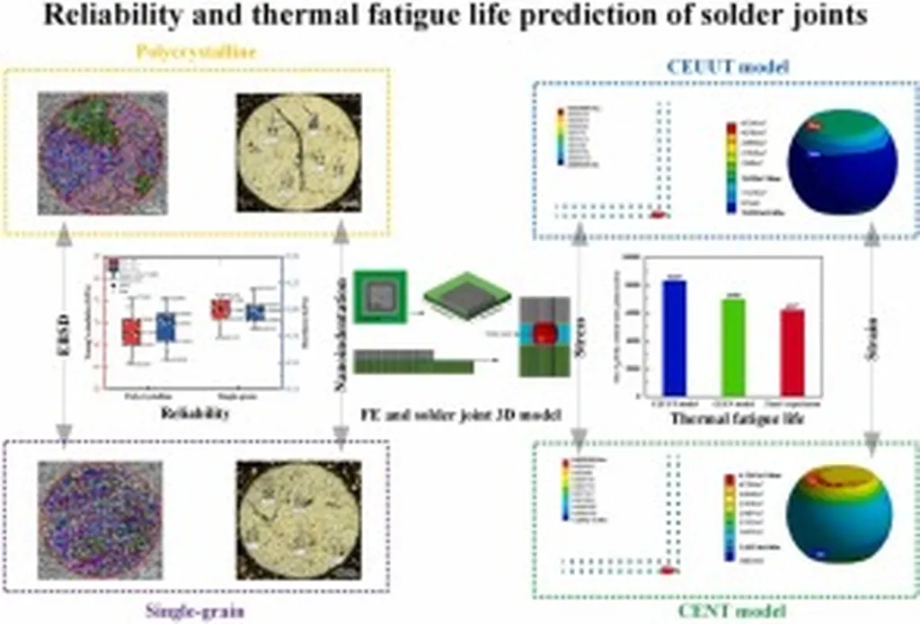
In the quest for more reliable and durable electronic packaging, researchers have turned to a tiny yet powerful tool: nanoindentation. This technique is helping scientists uncover the mechanical secrets of intermetallic compounds, which are crucial for the stability of solder joints in electronic devices. A recent study led by Wei-Rong Yang from the Academy of Circular Economy at National Chung Hsing University in Taiwan, published in the Journal of Advanced Joining Processes (translated as “Advanced Joining Processes Journal”), sheds light on how these compounds behave under mechanical stress, offering insights that could revolutionize the design of electronic interconnects.
Solder joints, the tiny connections that link electronic components, are often the weak points in electronic devices. They are subjected to mechanical stresses and thermal cycling, which can lead to failure. Intermetallic compounds (IMCs) form at these joints, and their mechanical properties are vital for the overall reliability of the device. However, understanding these properties at the nanoscale has been a challenge—until now.
Nanoindentation, a technique that applies controlled forces to extremely small areas, has emerged as a powerful tool for probing the mechanical properties of IMCs. In his study, Yang and his team used nanoindentation to investigate the hardness, Young’s modulus, plasticity, and creep resistance of various IMCs. They found that these properties depend significantly on the crystal orientation and structure of the compounds, as well as the alloying elements present.
“The nanoindentation technique allows us to measure the mechanical properties of IMCs with unprecedented precision,” Yang explained. “This level of detail is crucial for understanding how these compounds behave under real-world conditions and for designing more reliable electronic interconnects.”
One of the key findings of the study is the importance of the Young’s modulus-to-hardness ratio in evaluating the toughness and creep resistance of IMCs. This ratio can serve as a predictor of the long-term reliability of solder joints, helping engineers design materials that are more resistant to failure. The research also highlights the role of alloying elements in enhancing the mechanical properties of IMCs, offering a pathway to improving the durability of electronic packaging.
The implications of this research extend beyond the electronics industry. In the energy sector, where reliability is paramount, understanding the mechanical properties of IMCs can lead to more robust and long-lasting components for power electronics, renewable energy systems, and electric vehicles. As the demand for energy-efficient and sustainable technologies grows, the insights gained from this study could pave the way for more resilient and high-performance electronic interconnects.
“This research is a significant step forward in our understanding of IMCs and their role in electronic packaging,” Yang said. “By leveraging the nanoindentation technique, we can design materials that are not only stronger but also more reliable, ultimately contributing to the advancement of energy technologies.”
As the field of electronic packaging continues to evolve, the work of Yang and his team serves as a reminder of the power of nanoscale investigation. By delving deep into the mechanical properties of IMCs, researchers are unlocking new possibilities for enhancing the reliability and performance of electronic devices, with far-reaching implications for the energy sector and beyond. The study, published in the Journal of Advanced Joining Processes, marks a significant milestone in this ongoing quest for innovation and durability.

