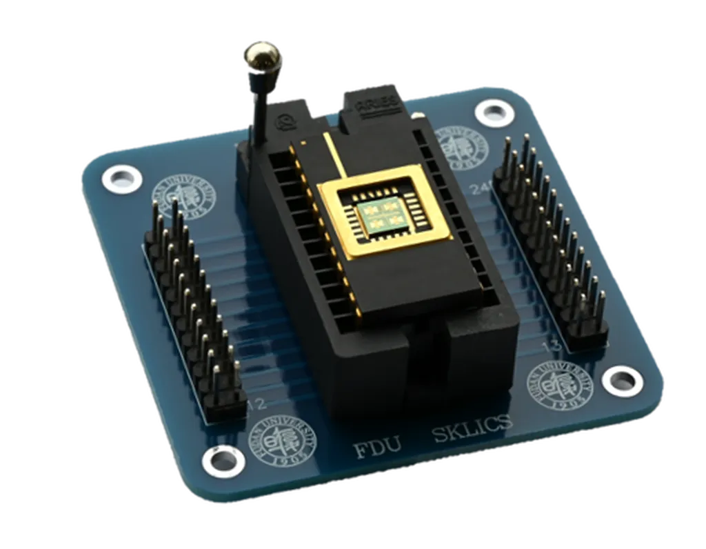
In the relentless pursuit of advancing semiconductor technology, researchers are increasingly turning to two-dimensional (2D) materials as a beacon of hope for the post-Moore era. A recent review published in *Information & Functional Materials* (translated from Chinese as *Information and Functional Materials*), led by Zhenggang Cai from the State Key Laboratory of ASIC and System at Fudan University in Shanghai, China, delves into the critical role of transfer technologies in integrating these 2D materials into next-generation electronics. The review, titled “The development of transfer technologies for advanced 2D circuits integration,” offers a comprehensive look at the methodologies and challenges associated with transferring 2D materials, a process that could revolutionize the electronics industry, including the energy sector.
The scaling limitations of conventional CMOS (Complementary Metal-Oxide-Semiconductor) technology have spurred the exploration of 2D materials as a transformative solution. These materials, just a few atoms thick, promise enhanced performance and new functionalities that could drive innovation in various applications, from flexible electronics to energy-efficient devices. However, the successful integration of 2D materials into practical devices hinges on the development of efficient transfer technologies.
Cai’s review meticulously examines both wet and dry transfer methods, highlighting the state-of-the-art techniques that enable high-quality, wafer-scale transfer of 2D materials. “The technology for transferring 2D materials is a crucial link between their synthesis and device integration,” Cai explains. “It’s essential to develop methods that are compatible with silicon lines while preserving the intrinsic properties of these materials.”
One of the key challenges discussed in the review is the need for massive transfer of 2D materials. This involves not only transferring the materials themselves but also integrating gate dielectrics and metal electrodes. The construction of van der Waals contacts at the 2D material/dielectric interface and the 2D material/metal electrode interface is particularly critical. These contacts are essential for ensuring the efficient operation of 2D devices, which could have significant implications for the energy sector. For instance, more efficient electronics could lead to reduced energy consumption in data centers, which are known for their high energy usage.
The review also explores the potential for layer-by-layer or tier-by-tier transfer of 2D devices for monolithic 3D integration. This approach could pave the way for the development of highly integrated, compact, and energy-efficient electronic systems. “The potential for monolithic 3D integration is immense,” Cai notes. “It could lead to devices that are not only more powerful but also more energy-efficient, which is a game-changer for the energy sector.”
Despite the promising advancements, the review concludes by highlighting the significant challenges that remain. These include leveraging the potential of 2D materials at the circuit and system levels and developing forward-looking strategies for transfer technologies. As the electronics industry continues to evolve, the insights provided by Cai’s review could shape future developments in the field, driving innovation and paving the way for a more sustainable and energy-efficient future.
The research published in *Information & Functional Materials* underscores the importance of transfer technologies in the integration of 2D materials. As the industry grapples with the scaling limitations of conventional technologies, the insights provided by Cai and his team could be instrumental in shaping the future of electronics, with far-reaching implications for the energy sector and beyond.

