In the ever-evolving landscape of optoelectronics, a groundbreaking study led by Jiale Wu from the Guangdong Engineering Research Center of Optoelectronic Functional Materials and Devices at South China Normal University has shed new light on the potential of gallium nitride (GaN) and two-dimensional (2D) materials. Published in *Information & Functional Materials* (which translates to *Information and Functional Materials* in English), the research delves into the fascinating world of heterojunction-based photodetectors, offering insights that could revolutionize the energy sector.
Photodetectors, devices that convert light into electrical signals, are crucial components in various applications, from renewable energy systems to telecommunications. The integration of GaN, a wide-bandgap semiconductor, with 2D materials, which are optoelectronically tunable and compatible with van der Waals forces, has opened up new avenues for enhancing photodetector performance. “Combining GaN with 2D materials allows us to control interfacial phenomena and unlock novel photodetection functionalities,” explains Wu. This synergy not only improves device mechanisms but also paves the way for innovative applications in the energy sector.
The study explores two primary techniques for integrating GaN with 2D materials: transfer and in situ growth. Each method has its unique impacts on interface quality and material compatibility. “The choice of technique significantly influences the optoelectronic behavior of the devices,” notes Wu. By tailoring the interface design, researchers can achieve functional diversity, making these heterostructures suitable for a wide range of practical applications.
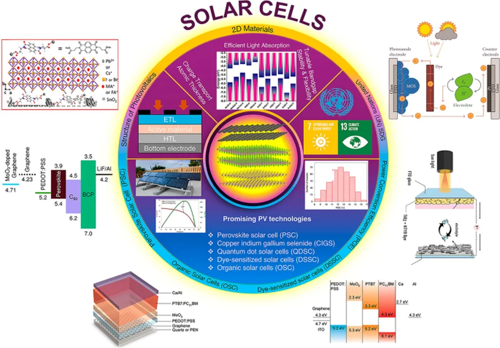
One of the most compelling aspects of this research is its potential to enhance the efficiency and functionality of photodetectors used in renewable energy systems. For instance, solar energy systems rely heavily on photodetectors to convert sunlight into usable energy. The integration of GaN/2D material heterojunctions could lead to more efficient and cost-effective solar cells, ultimately reducing the overall cost of solar energy.
Moreover, the study highlights the importance of band alignment and interlayer coupling in optimizing device performance. By understanding these fundamental aspects, researchers can develop high-performance intelligent optoelectronic systems that are not only efficient but also scalable. “Our findings provide a roadmap for future developments in the field,” says Wu. “We believe that these advancements will shape the next generation of optoelectronic devices, particularly in the energy sector.”
However, the journey is not without its challenges. The study identifies current hurdles in interface engineering, carrier dynamics, and scalable integration. Addressing these challenges will be crucial for realizing the full potential of GaN/2D material-based photodetectors. “While there are obstacles to overcome, the potential benefits are immense,” Wu acknowledges. “We are optimistic about the future of this technology and its impact on the energy sector.”
As the world continues to seek sustainable and efficient energy solutions, the research led by Jiale Wu offers a glimpse into a future where advanced photodetectors play a pivotal role. With its comprehensive overview of recent progress and insightful analysis of future directions, this study is a beacon of hope for the energy sector, promising a brighter and more efficient tomorrow.

